

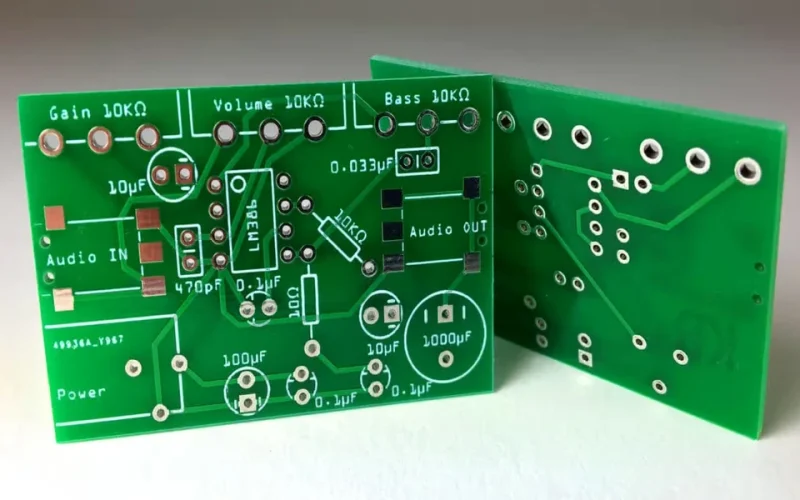
So you want to design your own printed circuit board. Maybe you’ve been building circuits on breadboards and you’re ready to make something permanent. Maybe you have a project idea that needs a custom board to work the way you want. Maybe you’ve just caught the hardware bug and you want to understand how the boards inside every device you own actually come to be.
Whatever brought you here, PCB design is one of the most rewarding skills a hardware enthusiast can pick up. The learning curve is real but not as steep as it looks from the outside, and the tools available today make it more accessible than it’s ever been. Here’s a grounded introduction to everything you need to know to get started.
What You’re Actually Doing When You Design a PCB
Before diving into tools and techniques, it helps to understand what PCB design actually involves at a high level. The process has two distinct phases that feed into each other.
The first phase is schematic capture. This is where you draw the logical circuit: which components are in the design, what their electrical properties are, and how they connect to each other. The schematic is the blueprint of the circuit. It doesn’t care about physical size, shape, or layout. It only cares about electrical relationships.
The second phase is layout. This is where you take the components from the schematic and arrange them on the actual physical board, then route copper traces between them to create the connections defined in the schematic. Layout is where the physical engineering happens: how big is the board, where do the components sit, how do the traces run, and how does it all fit together in a way that works electrically, thermally, and mechanically.
The output of the layout phase is a set of Gerber files, which are the files you send to a manufacturer to have the physical board made. Understanding that flow, schematic to layout to Gerber files to physical board, gives you a mental map of the whole process before you start.
Choosing Your EDA Software
EDA stands for Electronic Design Automation, and EDA software is the tool you use to do both schematic capture and PCB layout. Choosing the right one to start with matters because there’s a real learning investment involved, and switching tools partway through a project is painful.
The good news is that there are excellent free options for beginners that are also used professionally.
KiCad is the most widely recommended starting point for most beginners today. It’s free, open source, actively developed, has a large and helpful community, and is genuinely capable of handling professional designs. The interface has improved significantly in recent versions and the learning resources available, including tutorials, YouTube series, and community forums, are excellent.
EasyEDA is browser-based, which means no installation, and is tightly integrated with JLCPCB’s manufacturing and component ordering system. It’s a good choice if you want to get to a physical board as quickly as possible with minimal friction. The tradeoff is that it’s less capable than KiCad for complex designs and your project files live in the cloud.
Autodesk Eagle was the industry standard for small-team PCB design for many years and has a free tier for small boards. It has a large library of existing designs and tutorials but has been somewhat supplanted by KiCad in the hobbyist community since Autodesk moved it to a subscription model.
For most beginners, starting with KiCad is the right call. The initial learning curve is real but the payoff is a tool that will grow with you as your designs become more ambitious.
Your First Schematic: What to Know
Opening a schematic editor for the first time can feel overwhelming because the interface has a lot of options. The core workflow is actually straightforward once you understand what you’re doing.
You place component symbols from a library onto the schematic canvas and draw wires between their pins to define the electrical connections. Component symbols are abstract representations, not physical shapes. A resistor symbol is two lines with a rectangle or zigzag between them regardless of whether the physical component is a tiny SMD part or a large through-hole resistor.
A few fundamental concepts to understand before you start:
Nets are named electrical connections. Every wire in your schematic belongs to a net, and every component pin connected to that wire shares the same net. The net named VCC and the net named GND are special: they represent your power supply rails and ground reference respectively. Naming nets is important because the layout tool uses net names to know which pads should be connected by traces.
Power symbols let you connect component pins to power and ground without drawing wires across the whole schematic. Instead of running a wire from the positive supply pin of your voltage regulator all the way to the power pin of every IC, you place a VCC symbol on each pin and the software understands they’re all connected.
Component values need to be set for passive components. A resistor symbol needs to know it’s a 10k resistor. A capacitor symbol needs to know it’s 100nF. These values travel through to the bill of materials and to the layout.
Run the electrical rules check (ERC) when your schematic is complete. It catches unconnected pins, missing power connections, and other common errors before you move to layout.
Understanding Footprints
This is where a lot of beginners get tripped up for the first time, so it’s worth paying close attention.
A component in your EDA tool has two parts: the schematic symbol, which represents the component electrically, and the footprint, which represents the component physically on the PCB. The footprint defines the size and position of the pads that you’ll solder the physical component to, along with a courtyard boundary showing how much space the component occupies.
The most common beginner mistake is choosing a footprint that doesn’t match the physical component you plan to use. A resistor might come in half a dozen different SMD package sizes (0402, 0603, 0805, 1206) and the pads for each are a different size and spacing. If you assign the wrong footprint, the physical component won’t fit the pads on the manufactured board.
Before you finalise your layout, cross-reference every footprint against the datasheet for the actual component you plan to solder. This is tedious but critical. A board that comes back from fabrication with a footprint mismatch needs a respin, and that costs both time and money.
Layout Fundamentals
Moving from schematic to layout for the first time is a moment that either excites or overwhelms most beginners. The canvas shows your components as physical footprints connected by thin lines called ratsnest lines, which represent the connections that need to become copper traces. Your job is to arrange the components sensibly and route those connections.
A few principles that will serve you well from the start:
Component placement first, routing second. Spend real time getting your component placement right before you draw a single trace. Good placement makes routing easier and often makes the difference between a board that works well electrically and one that causes subtle problems. Place components that connect to each other close together. Orient connectors toward the edge of the board. Keep your power supply components in their own area.
Route power and ground first. Power and ground connections affect every part of the circuit. Getting them right before routing signals means you’re building on a solid foundation. On a 2 layer board, use a ground pour on the bottom layer to create a ground plane rather than routing individual ground traces.
Keep traces short and direct. A trace is a wire, and longer wires have more resistance and inductance. For signal traces, shorter is almost always better. Route the most critical signals first and give them the most direct paths.
Follow your design rules. Your EDA tool has design rule settings that define minimum trace widths, minimum clearances, and other manufacturing constraints. Set these to match your manufacturer’s published capabilities before you start routing and run the design rule check (DRC) regularly as you work. Catching violations during layout is much easier than fixing them all at the end.
Getting Your Board Made
Once your layout is complete and your DRC is clean, you generate Gerber files and send them to a PCB manufacturer. For beginners, the major online prototype fabs make this process remarkably accessible. You upload your files, configure your board parameters (size, layers, surface finish, quantity), pay, and wait.
For first boards, standard parameters keep costs low and avoid complications: 2 layers, 1.6mm thickness, HASL surface finish, green solder mask, and white silkscreen. Most beginner designs work perfectly well with these defaults.
Manufacturers like Avanti Circuits are worth knowing about for when your projects grow beyond simple prototypes and you need more capability, tighter tolerances, or faster domestic turnaround. As your designs become more demanding, the manufacturer you choose starts to matter more, and having options beyond the entry-level online fabs gives you more flexibility.
Before you submit anywhere, open your Gerber files in a free online Gerber viewer and check every layer visually. Confirm the copper looks right, the board outline is correct, and there are no obvious missing layers or mirrored geometry. This five-minute check has saved countless designers from ordering boards with avoidable errors.
When Your First Board Arrives
Getting your first self-designed PCB back from a manufacturer is a genuinely exciting moment. Before you solder anything, do a quick visual inspection: check the board dimensions, look at the solder mask coverage, and confirm the silkscreen is legible.
Then go slowly. Solder one section at a time and test as you go rather than assembling the whole board and powering it up hoping for the best. Start with the power supply circuit and verify your voltage rails before populating anything else. A power fault that’s caught before other components are installed saves those components from potential damage.
When something doesn’t work as expected, and something almost always doesn’t on a first board, approach debugging systematically. Check your schematic against your layout. Check your component values. Check your footprint orientations. Most first-board problems come down to one of a handful of common issues: a backwards component, a missing connection that was in the schematic but didn’t make it to the layout correctly, or a component value that was set wrong.
The Learning Mindset
Every experienced PCB designer has a collection of first-board failures, respins they’d rather forget, and components that were backwards or the wrong package. Those experiences are how the knowledge gets built. The goal of your first board isn’t a perfect board. It’s a board that teaches you something.
Keep your first designs simple. A board that does one thing clearly is much better for learning than an ambitious design with many subsystems, because when something goes wrong you have fewer variables to investigate. As you get comfortable with the process, add complexity gradually.
Take notes on what went wrong and why. Those notes become your personal design checklist and they get more valuable with every board you spin.
The Bottom Line
PCB design is a skill that builds quickly once you start. The concepts are logical, the tools are accessible, and the feedback loop of designing a board, ordering it, assembling it, and seeing it work is one of the most satisfying in all of hardware development.
Start with KiCad, start with a simple design, take your time on component placement, and don’t be discouraged when your first board needs a revision. Every board you spin makes the next one faster and better. That’s the process, and it works.
